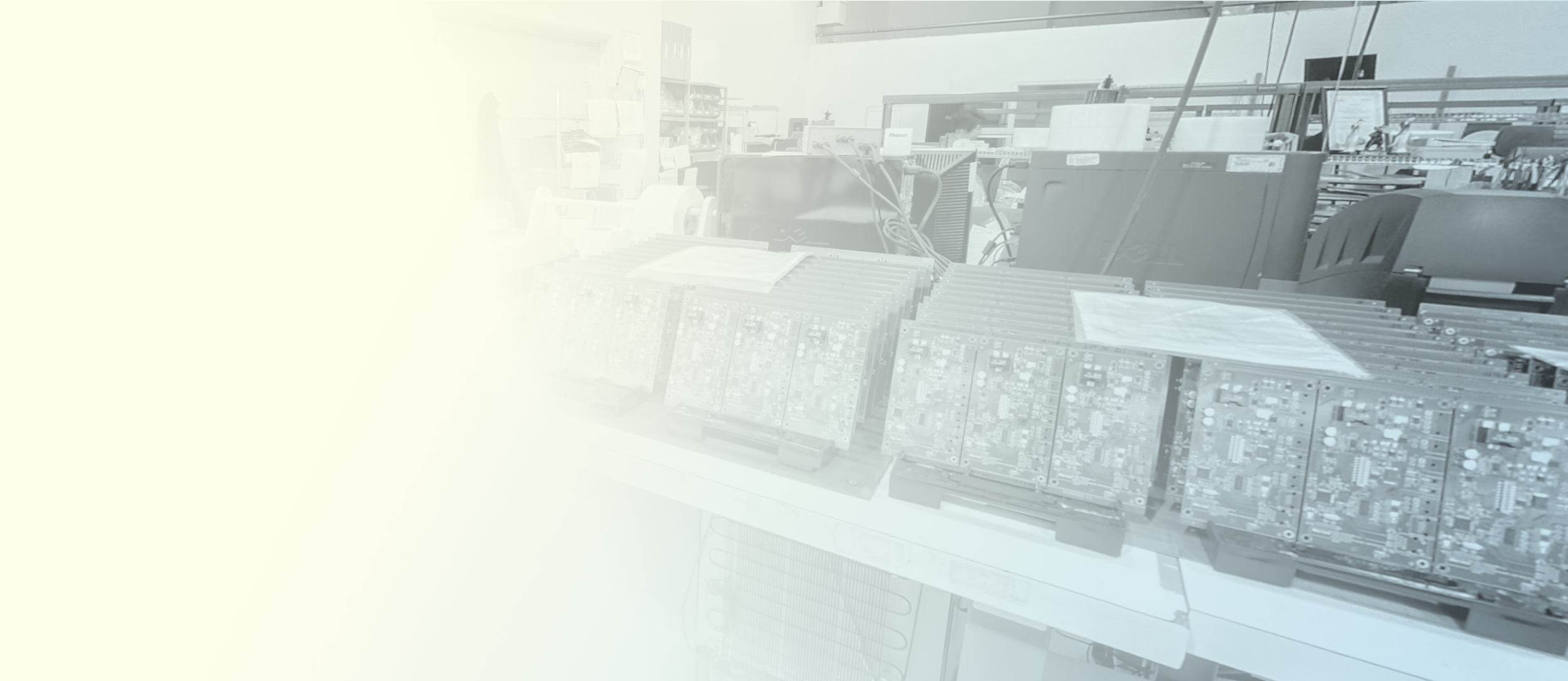
Circuit boards are electronic hardware that consist of electrical or data circuits placed on a flat base material. Traditionally, industrial professionals employed point-to-point construction to manufacture circuits boards. However, with the development and introduction of printed circuit boards (PCBs), they began using other manufacturing methods, such as chemical etching, laser processing, and milling, to “print” the circuits, creating pathways through which electricity can travel.
The first contemporary PCB was created by Paul Eisler in 1936 for a radio system. However, PCBs only found use in general production applications in the last few decades. This growth trend can be largely attributed to developments in electrical and circuitry technology, which have allowed designers and engineers to condense circuits onto smaller surface areas by using the space more efficiently and designing them in three dimensions.
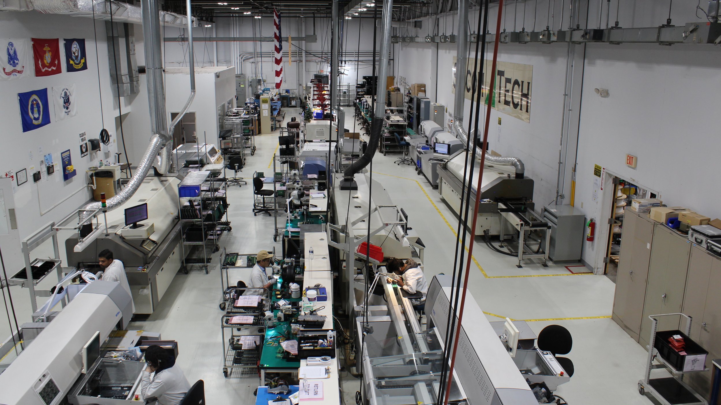
Syscom Tech is an industry-leading contract manufacturer providing full turnkey solutions for a diverse set of industries, including printed circuit board assembly services. Equipped with state-of-the-art assembly, inspection equipment and astute quality control procedures, we create simple to complex PCB assemblies in prototype to high-volume production runs with the highest level of quality possible.
Applications of Printed Circuit Boards
PCBs—also referred to printed circuit board assemblies (PCBAs) when integrated with electronic components—find application in virtually every modern electronic device available in the market. Some of the most common devices they are found in include:
-
Computers
-
Industrial machinery
-
Medical devices
-
Consumer electronics
-
Smart or LED lighting
What are Some Advantages of PCBs?
Printed circuit boards offer several advantages, such as:
-
Small footprint. The invention and adoption of PCBs have allowed industry professionals to produce smaller, more compact electronic circuits. This quality allows for more powerful electronic devices without increasing their size.
-
Faster production time and great scalability. PCBs can be produced quick and production can be scaled to meet the demand for small and large orders. When manufactured in large quantities, the cost-per-unit is much lower.
-
Excellent performance. PCBs don’t have parts that can become loose, have failed connections, or short circuit. Additionally, their performance stays consistent regardless of movement, which is ideal for mobile devices, and they have low levels of electronic noise.
Five Common Types of Printed Circuit Boards
Printed circuit boards are available in a wide range of designs and configurations. Five of the most commonly employed types include:
1. Single-Layer PCBs
Single-layer—i.e., single-sided—PCBs are made out of a single base material (i.e., substrate) that is then coated in a thin layer of metal—typically copper—and a solder mask. Manufacturers etch and apply electronic components to only one side of the circuit board. These PCBs are easy to produce and have a very low cost, especially when manufactured in large quantities. They are the most commonly used type of PCB, finding use in consumer, commercial, and industrial electronic equipment.
2. Double-Layer PCBs
Double-layer—i.e., double-sided—PCBs have the same basic makeup as single-layer printed circuit boards, but they have circuits and other components on both sides of the boards. Vias (i.e., channels) running through the board allow circuits on one side of the board to communicate with parts on the other side of the board. These PCBs increase the amount of functional surface area available for circuits without increasing the amount of physical space needed.
Applications for double-layer PCBs generally involve electronic devices that need intermediate or complex circuit systems without increasing the size of the equipment, such as automotive dashboards, vending machines, and HVAC systems.
3. Multi-Layer PCBs
Multi-layer PCBs have three or more laminated between the external layers of the solder mask. The use of insulation prevents the buildup of excessive heat that can melt sensitive components. This type of PCB ranges in the level of complexity—from 4 to 50 layers in thickness—and can accommodate complex and complicated tasks. Applications include data storage, GPS devices, satellite systems, and complex medical equipment.
4. Flexible PCBs
In contrast to rigid PCBs, flexible PCBs are made to move and flex. They are made from flexible materials, such as plastic, and are available in single-layer, double-layer, and multi-layer variations.
Compared to rigid PCBs, these printed circuit boards offer several advantages. For example, their greater flexibility allows for their use in spaces that require folding over edges or wrapping around corners. This flexibility can result in significant cost and part weight savings, as a single flexible PCB can be used in place of multiple rigid PCBs. Additionally, flexible PCBs can be built with materials that enhance waterproof, shockproof, corrosion resistance, and other advantageous characteristics, making them better suited for a broader range of environmental conditions. However, as their manufacture necessitates printing on a flexible material, the cost of production tends to be higher than that of rigid PCBs.
5. Rigid-Flex PCBs
Rigid-flex PCBs are a hybrid of rigid and flexible circuit boards. Each unit contains a combination of flexible and rigid PCB layers, which reduces the number of boards needed to meet wiring requirements and allows device designers to create more streamlined designs with fewer parts or space considerations. Applications for rigid-flex PCBs generally involve part or product designs with space or weight restrictions, such as automobiles, cellphones, and medical devices.
Partnering With Syscom Tech for High-Quality PCB Assembly Solutions
Syscom Tech is an AS9100D certified and RoHS compliant company specializing in the high-quality manufacturing of printed circuit boards (PCBs) through assembly and delivery. For every project we take on, we implement comprehensive quality control measures so you and your customers can rely on each circuit’s performance. Some of the equipment we employ includes:
-
Automatic optical inspection (AOI) camera for inspection of components accurate to 5 microns
-
SMT pick & place equipment for complete accuracy during assembly with dimensions of up to 20 inches by 20 inches
-
X-ray inspection system for real-time inspection of BGA components for voiding, positioning, and solder joint integrity